6. Execution unit
Phases of instruction execution
To execute an instruction, the processor must:
read (fetch) it from memory hierarchy
decode it
read the source arguments if needed
perform an arithmetic/logic/other operation
write the result (if needed)
There phases may be mapped into:
- Different parts of combinatorial login, operating in a single clock cycle - single-cycle computer
- Different clock cycles of a microprogrammed devices - multicycle processor
- Different parts of combinatorial operating in different clock cycles - pipelined computer
Single-cycle implementation of RISC-V
Sequential circuit which changes its state once during the instruction execution
The instruction is executed in a combinatorial circuit
Assumptions for model processor:
- Simplified RISC-V model
- Harvard architecture:
distinct program and data memories
program memory is a Read-Only Memory - All instructions are 32 bits long, stored in 32-bit wide memory
- Sequence of actions is the same for all instructions
some actions may not be needed in some instructions - may be skipped but not reordered - Byte memory addressing - word only access.
data and instructions are size-alignment
Instruction fetch
PC value used as program memory address
incremented by 4 - nextPC
current PC value used by branches
Instruction word available at the output of instruction memory
Single-cycle processor control unit
Control unit
Parts of instruction word are supplied to the inputs of a control unit
Control unit produces signals used to control all other blocks of processor
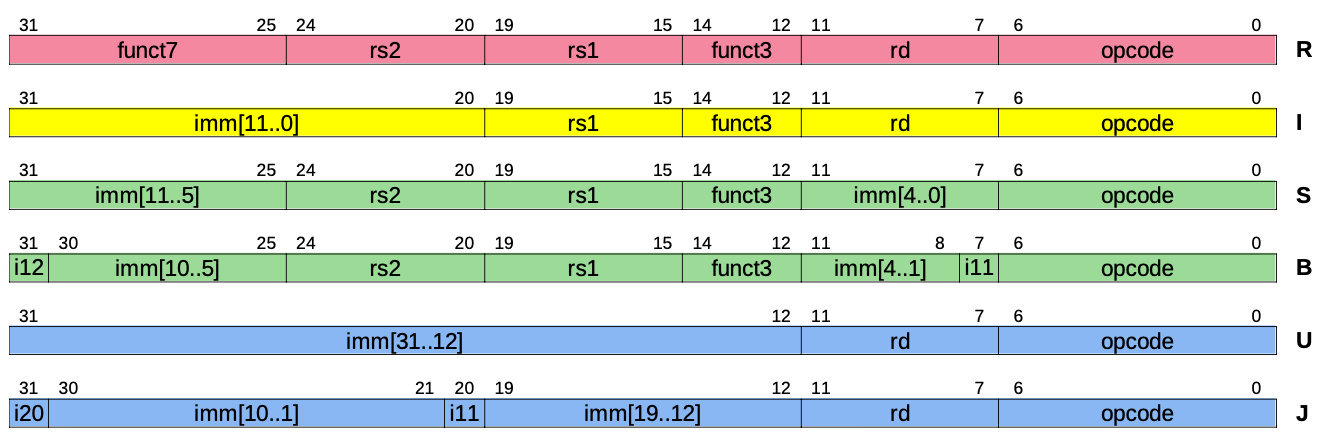
Instruction formats

Argument fetch
Register source arguments
- Rs
- Rt (in all R format instr. and in some I format instr.)
Immediate argument (I format) - obtained by extending the 16-bit constant field to 32-bits in data extender Ext
arithmetic instructions, branches, memory references
logical instructions
Second argument selected using Mux_ALU depends on instruction
Destination register number (if used) comes from Rt or Rd field
Schema

ALU, branch
ALU - Arithmetic Logic Unit - performs the operation according to currently executing instruction
Adds the base register and displacement to get memory address
During branches, performs compare operation to obtain the logical value of relation - output on COND
Outputs 4-bit ALU operation code and 5 control signals
- Branch - active during conditional branch instructions
- Load - controls final data result multiplexer
- Store - enables memory write, selects alternate immediate field multiplexing
- Register Write Enable - active during arithmetic/logic and Load instructions
- Immediate - active during I- and S- format instructions
ALU operations:
ADD, SUB, SLT, SLTU, SLL, SRL, SRA, AND, OR, XOR
ALU operation is set to ADD for instructions other than arithmetic
during loads and stores - ALU sums the base register and displacement to form the memory address
During branch instructions, signal used for ALU function selects the proper branch condition output
ALU argument selections
First source argument is always rs1 register conent
Second source argument may be rs2 or immediate
ALU, data memory, branching

Data memory
Data memory module is idle during all instructions other than loads and stored
ALU output is used as memory address
Access
During stores, Rt register content is stored to memory
During loads, data from memory is stored to Rt
Control path
The control path (at the top of schematic) generates the PC value for the next subsequent instruction
PC adder produces the possible branch target address by adding the current PC value and branch displacement
Branch multiplexer selects between nextPC and branch target
branch target is used when current instruction is conditional branch and the condition is true
Finalizing the instruction
Three possible results
- newPC value for subsequent instruction (always)
- data to be written to the rd reg (during arith/logic and loads)
- data to be written to memory during Store
Result select multiplexer selects the output value
Clock edge stores the results in their respective destinations
this causes PC update and starts the next instruction
RV32I instruction formats
Presented model limitations
For basic HHL support, JALR (I-format) is missing
JALR may be used for procedure calls and returns
Other application instructions missing (U- and J- format)
- LUI - loading long constants
- AUIPC - loading PC-relative addresses
- JAL - unconditional jump or procedure call with 21-bit displacement
Single-cycle design limitations
Harvard architecture - instruction memory is read-only
Fixed order of actions within instructions
- instruction fetch
- decode/read registers/prepare constant
- compute result/data memory address, compute branch target
- data memory access
- store the result in a register
Simple programming model
memory data cannot be directly used as argument
Problems
Separate memories - high cost, large size, lack of programmability
Multiple expensive units - three adders (PC, ALU, branch adder)
Low efficiency
Solutions:
- earlier - multicycle implementation
- today - pipelined architectures
Multicycle processor
Minimizes the number of functional blocks by using the same block multiple times during the execution of one instruction
Requires breaking the execution into several phases (cycles)
in every phase every block is used for a different task
number of phases range from 2 to 10
Execution is controlled by a complex control unit implemented as synchronous automate
Number of multiplexers is increased due to the increased number of data paths and complexity of data flow
Unified program and data memory
- Princeton architecture
- Programmability
- Memory may be accessed 2/3 times during single instruction
Multiple use of ALU - PC incrementation
- Arithmetic operation
- Branch target address computation
Multiphase execution requires the instruction binary image to be stored in a register
Special Instruction Register in the Control Unit
Analysis
Execution of a single instruction requires several operations
General sequence of execution phases:
- Instruction fetch
- Instruction decoding
- Argument read
- Execution (ALU result)
- Result write
Multicycle processors usually implement CISC model
Structure
Memory is placed externally to the processor and is connected to processor using so-called bus
The processor is interfaced to memory via the bus interface unit places inside the processor structore
Processor functional units:
- Control unit
- Register set
- ALU
- Bus interface unit
Operation
During various phases of execution, only some of functional blocks are active
Instruction fetch - bus
Instruction decoding - control unit
Argument read - register set or bus
Execution - ALU
Result store - register set or bus
Most units remain idle for most time
Phases of instruction cycle are called machine cycles
Single machine cycle may required multiple clock cycles
Optimization
Number of machine cycles depends on internal data transfer capabilities of the processor
Number of machine cycles and clock cycles may be reduced by introducing extra data buses inside the processor
Instruction fetch optimization
We can improve overall performance, by fetching the next instruction while still executing current one
Instruction prefetch
Implementation - new elements needed, places in bus interface unit
- extra PC register scanPC
- prefetch register storing the instruction fetched in advance
Operation - when the bus is idle (decode phase) and prefetch register is empty, bus fetches next instruction in advance, using address stored in scanPC and increments scanPC
- Control unit may skip the subsequent fetch phase and start decoding immediately after writing the result of the previous instruction.
This way, we can skip fetch phase in most cases
Problems
In CISC, the instructions vary in length
After branch, scanPC value differs from nextPC, as it contains the word fetched from the address following the branch
Instruction queue
Solution to problem caused by CISC having various-length instructions
FIFO buffer instead of single prefetch
After every taken branch the queue contents must be invalidated and nextPC must to copied to scanPC
Branch penalty problem
As the fetch phase cannot be skipped following a taken branch, the instruction at branch target executes slower than other instructions
This difference in execution time is called branch penalty
Statistically branches constitute 7-14% of all instructions
making this a serious cause of efficiency reduction

Decomposition of single-cycle processor
Single-cycle to pipeline
D-type registers are places on cut lines
Instruction execution
- When PC changes, all signal values are stored in the register by supplying the clock edge to register's clock input
- After signals from D register output propagate, the state of signals is stored in the next D register
- After signals from last block propagate to the inputs of PC and register set write port, clock edge is supplied to PC and register set
Signal flow remains unchanged, only 4 registers were added
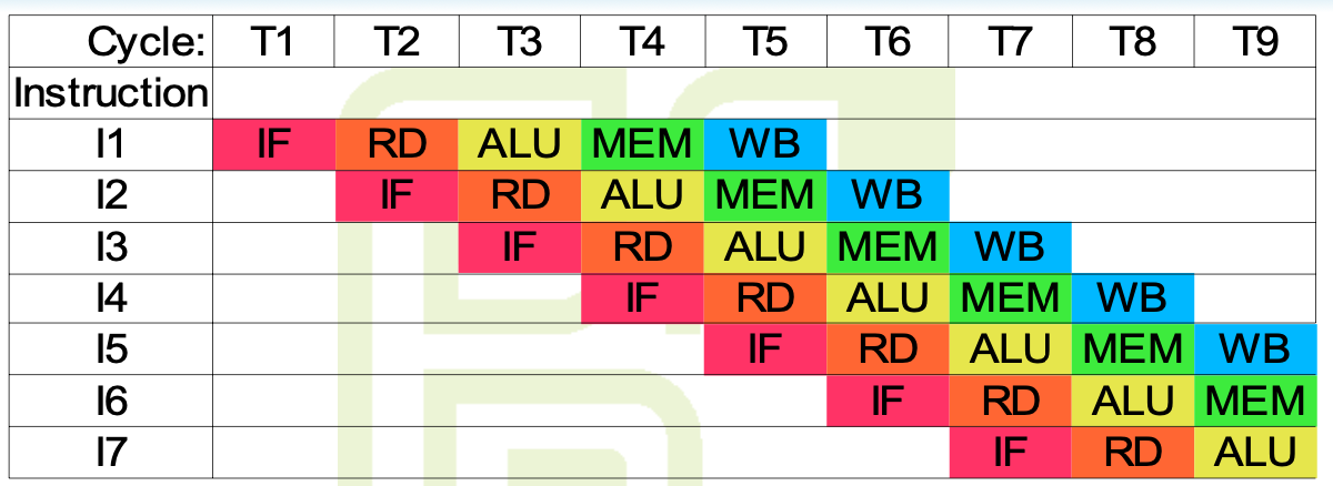
Execution of a single instruction requires 5 clock phases
much shorter than in single-cycle solution
Every cycle a new instruction is started one instruction is completed
Externally - one instruction per cycle
Example pipeline structure stages
- IF (instruction fetch)
- RD (read) - instruction decode and read source arguments
- ALU
- MEM (memory) - data memory load or store
- WB (write back) - write result to register