Fundamentals of Logic Circuit Design
Combinatorial Logic
Logic circuits are electronic circuits processing two-valued signals. Their operations are described by logic functions (Boolean algebra).
Boolean algebra
Laws
Truth table
| x | y | x+y |
|---|---|---|
| 0 | 0 | 0 |
| 0 | 1 | 1 |
| 1 | 0 | 1 |
| 1 | 1 | 1 |
Commutative Law
Distributive Law
Absorptive Law
Useful
de Morgan's Laws
Examples
1
2
3
4
Basic gates
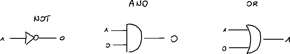
Typical gates have
In case of the AND gate, the rest 3 inputs need to be connected to 1
Algebraic manipulation of expressions can lead to the reduction of the circuit size
NOT and OR are the most basic gates
we can create any possible circuit using only NAND gates, or NOR gates.
Useful expressions:
Logic function minimalization
Gray's Code
The idea of Gray's code is that the consecutive states differ only by one bit, not the value of the bits
3 bit
000
001
011
010
110
111
101
100
4 bits
0000
0001
0011
0010
0110
0111
0101
0100
1100
1101
1111
1110
1010
1011
1001
1000
General idea of absorption law is that it works on pairs only.
But we can technically make it work on bigger sets.
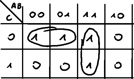
Karnaugh tables
Sum of products
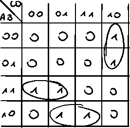
Top row and left column contain inputs, and middle of the table contains every possible output.
How to solve - Sum of Products
We're interested in which inputs give ur output 1
We circle 1's together (groups of 2, 4, 8...)
Those groups can be in line, in a square, or made by 'jumping' from one edge of another (think like snake game)
Then, we check which inputs change on those outputs, and we eliminate them, so we're left only with static inputs for given outputs
So for the top right 'island' - B changes, A, C and D are static.
Now, we write AND of all those inputs, so for our island it will be
For most-left island -
Bottom island -
So the whole output function will be
To remember
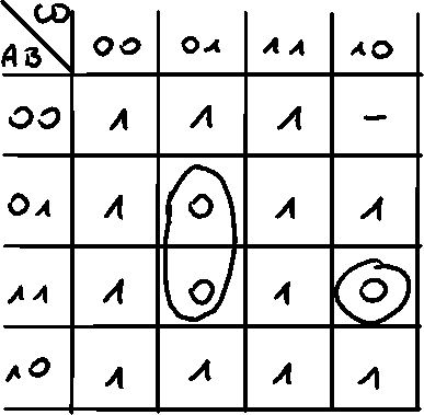
Sometimes, we don't need all outputs that we have available (explained in the beginning of Basic gates)
In that case, we put '-' instead of a output in the Karnaugh table. This is called a DONTCARE
When solving K-maps, when we circle DONTCARE, it gets turned
into 1, if not - into 0.
Thanks to that, DONTCAREs can be used like 'blanks' in scrabble
Product of sums
Quine McCluskey method
Computer software way of solving boolean algebra
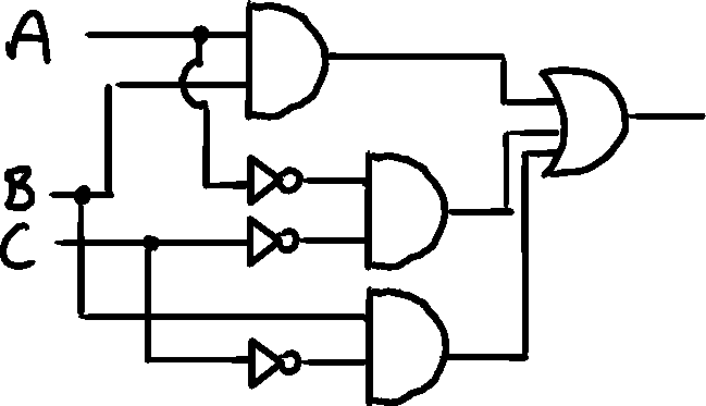
Static hazards
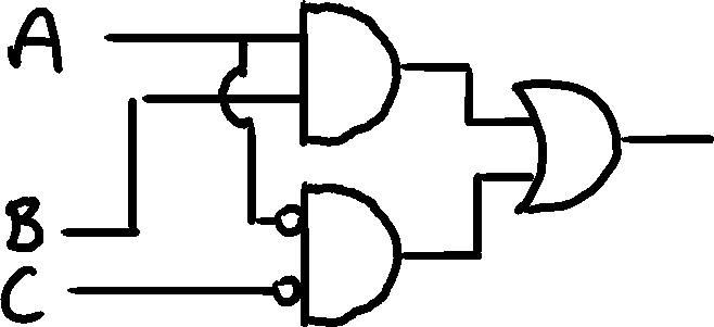
A static hazard it present for two neighboring 1's that aren't in the same minterms
When transitioning from a state 110 into 010
But to correctly show the steps, we need to split the diagram into stages.
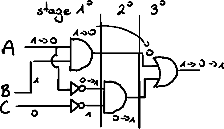
When switching from 110 to 010, the top AND gate gets updated at the same time as bottom NOT gates, but because the bottom signal has to travel also through an AND gates, the final OR gets a split moment signal, where the top input is already updated, but the bottom didn't catch up yet. This is called a static hazard.
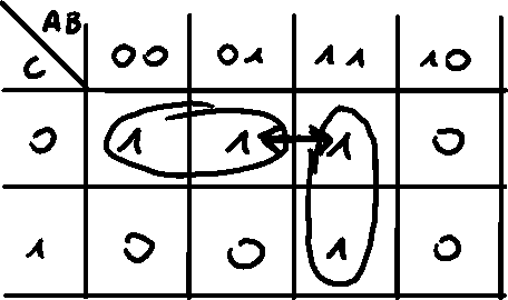
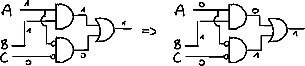
Fix
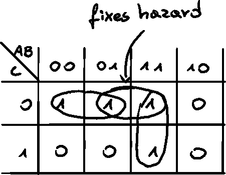
To fix the hazard, we can find the edge on the K-map that creates the problem and create a minterm from the 1's. This introduces a new part of the circuit that ensured the proper functioning of the whole circuit.
K-map
Updated circuit